Custom Machining Pot & Plunger for Semiconductor Packaging
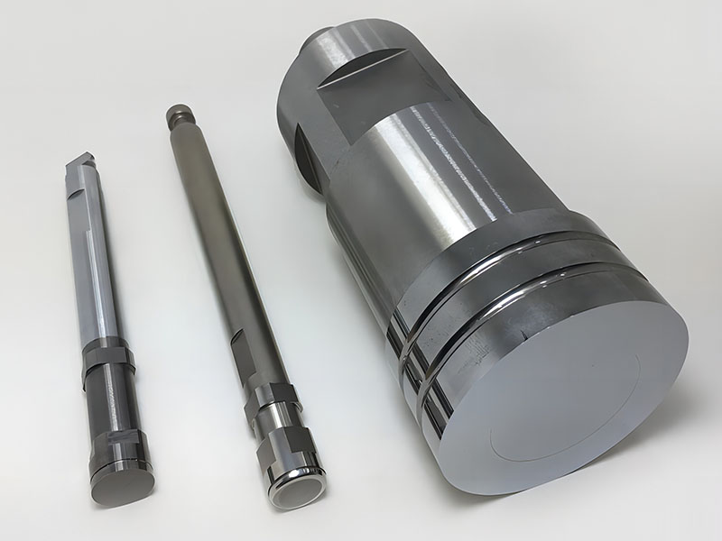
The company is one of the largest manufacturers of Pot & Plunger in China and we provide OEM services for Pot & Plunger to well-known semiconductor companies in China and Taiwan.
Pot & Plunger is used in the manufacture of semiconductor packaging moulds. The company's Pot & Plunger can be manufactured using M42 high speed steel or tungsten carbide and can also be supplied with additional PVD coating services.IC Package Mold Parts Cavities and Inserts
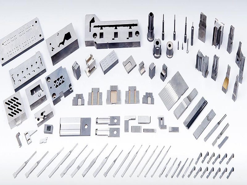
We offer fabrication and customization services for semiconductor die components, including:
-IC encapsulation die cavities and inserts
-IC leadframe stamping die punches and bushings
-Semiconductor packaging die plungers and pots, -Semiconductor packaging die plungers and pots
-Encapsulation die cores and core pinsMaterials: tungsten carbide, technical ceramics, tool steel, HSS, ASP23, etc.
Semiconductor Leadframe Mould & Die Tooling Machining
Semiconductor leadframe moulding A metal substrate that serves as a lead to connect a semiconductor chip to external circuitry and as a frame to hold a semiconductor package to a circuit board.
As a key component of a semiconductor integrated circuit, it is connected to the chip by thin leads and transmits electrical signals between the semiconductor chip and the substrate, and acts as a frame to protect and support the chip from external moisture or shocks.


