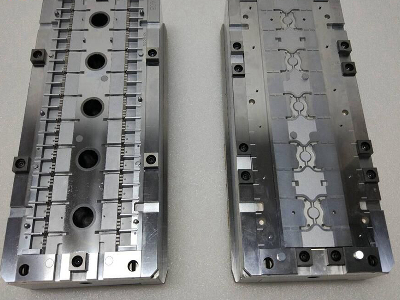
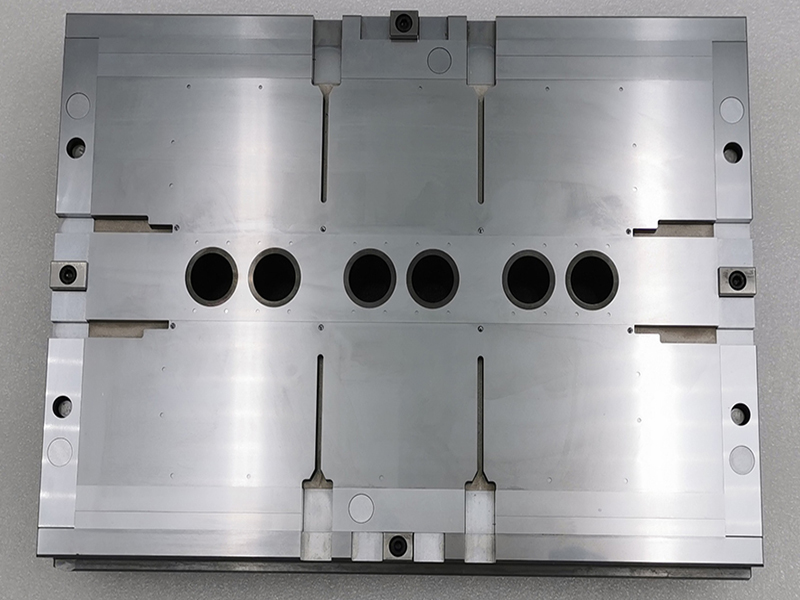
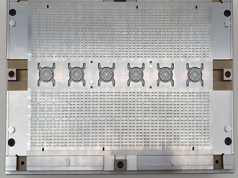
IC Packaging Mold Cavity Bar and Auto Mold Chase
Application: Suitable for TOWA, FICO, ASM, HANMI brand AUTO MOLD SYSTEM
Can be used in conjunction with automatic encapsulation systems to improve the intrinsic quality of the product.
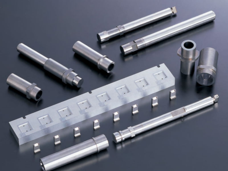
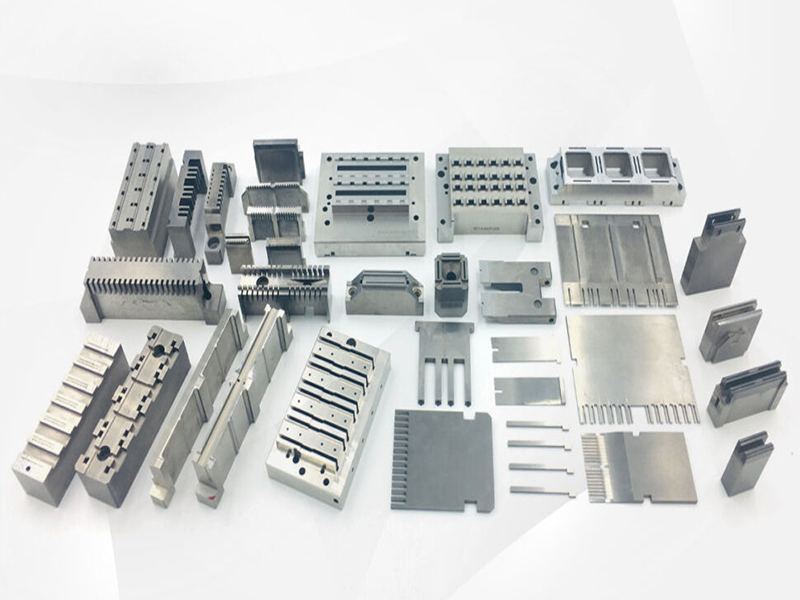
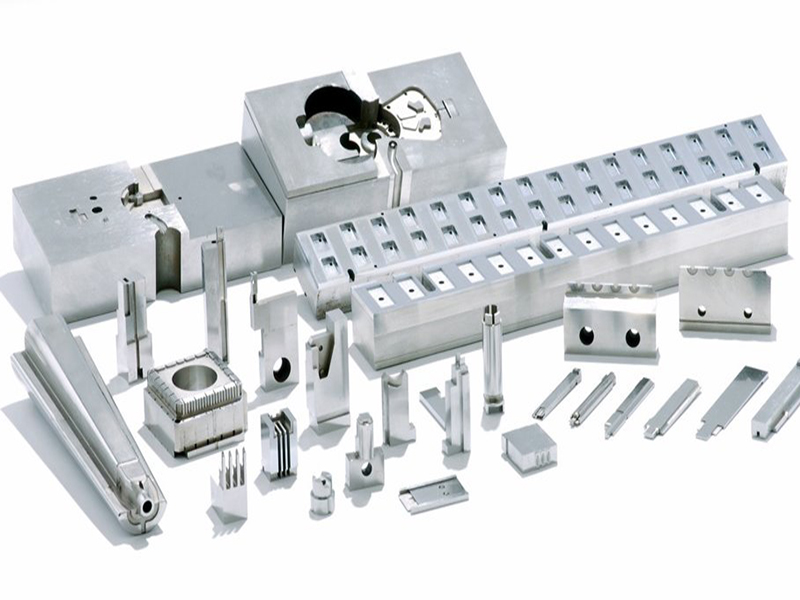
We manufacture AUTO MOLD for semiconductor packaging moulds and offer the manufacture of special parts for moulds.
-MOLD CHASE
-IC packing molds
-Cavity bar
-BTM cavity block
-DIP sliding cover
-Runner plate
-Base of BTM cavtiy bar
-Auto mold chase
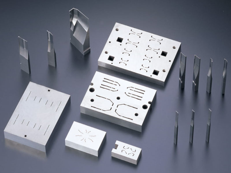
-QFN package mold insert
-Molded insert TO247
-SOT mold for semiconductor packaging
-Molded insert for semiconductor packaging die (top)
-Forming cavity (insert) under semiconductor package
-Mould inserts
-Molded insert in semiconductor package (TO92)
-Die box for mould sealing of semiconductor and integrated circuit
-Semiconductor gate runner mold
-Gate runner mold etc.
Manufacture of semiconductor tools from drawings
Semiconductor Manufacturing
Related products
OEM/ODM Punches and IC Die Pins for Semiconductors
Precision stamping die components are used in the semiconductor field. Punches and IC die pins are finished with tungsten carbide or hardened tool steel, and additional PVD coating services are also available. SPP INDUSTRY's die components are 6 times more durable than ordinary die standard parts, which is one of our patented products.
Pot,Plunger, Gate Insert for Semiconductor Dies
We have customized IC die pins for semiconductor test equipment (IC testers) and our highest priority is to provide our customers with comprehensive technical, engineering and manufacturing support for all your connection needs.
We also offer the widest range of suction cups for your automation solutions. Including custom suction cups to fit your specific application.
-pot, plunger
-gate insert
-punches and pins
Semiconductor Components and Tooling Manufacturer
We are a manufacturer of semiconductor components and tooling, providing high precision OEM parts services, including tungsten carbide punches, package mold cartridges and plungers, leadframe stamping mold parts, IC hot runner gate parts, etc.
Lead Frame Tooling & Stamping Die Parts
SPP INDUSTRY manufactures a variety of leadframes using ultra-precision tooling by stamping and etching, and provides OEM services for high-precision tooling components.

SPP Industry Ltd.
In the 1990s, SPP Industry Ltd was one of the first manufacturers to establish CNC machining in China. The company has now established five major machine parks in China, with significant achievements in the areas of 5-axis machining, precision grinding & honing, gear machining, large parts machining, custom tungsten carbide and new material development respectively.


